![[SW flag]](pic/Sw_flag_40.png)

![[UK/US flag]](pic/UK-US_flag_40.png)

|
|

Design of an H BridgeDesign of an H bridge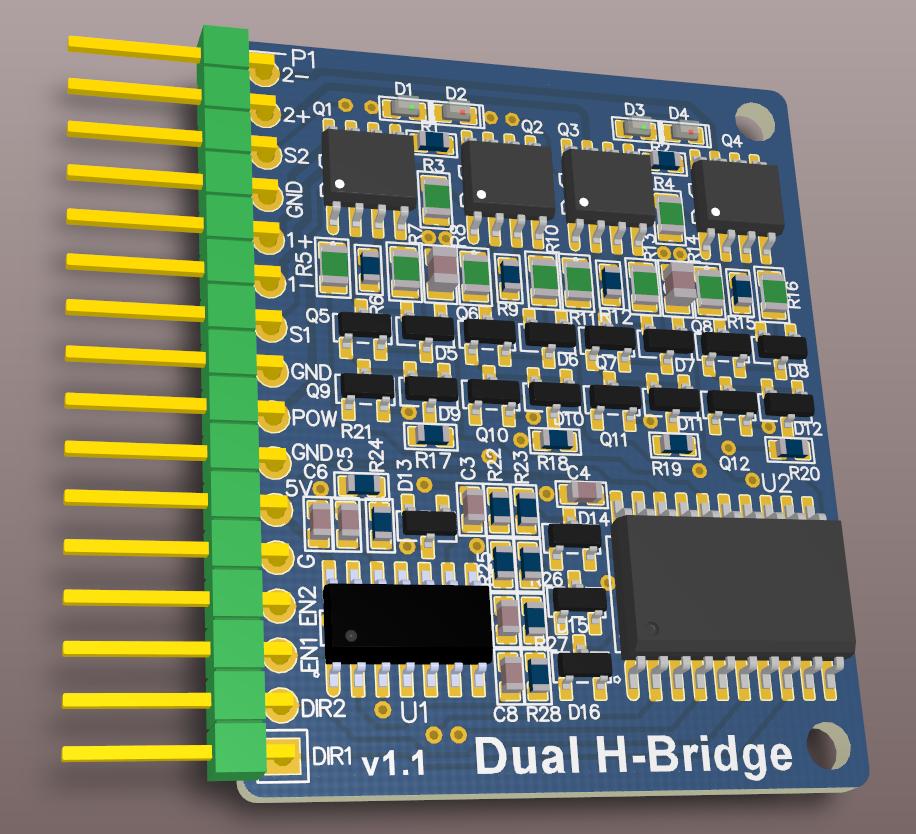
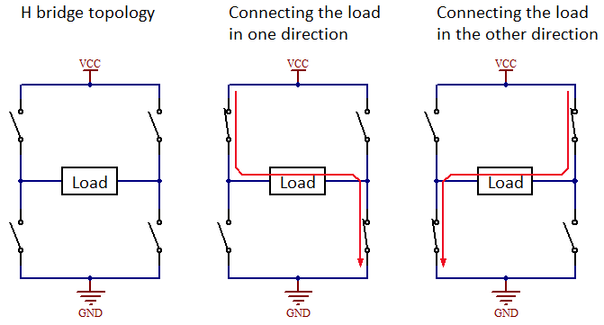
An "H bridge" is a circuit that can connect a supply voltage to a load in either direction. Typical usages of an H bridge are to drive a DC-motor forwards or backwards or to drive the windings of bipolar stepper motors. They find extensive use in robotics and other areas where motors or solenoids need to be controlled. Wikipedia has some more background information about H bridges, http://en.wikipedia.org/wiki/H-bridge. Figure 1 below shows the basic topology of an H bridge. The reason for the name of the circuit should be obvious from the figure.
Figure 1. Topology and basic operation of an H bridge.
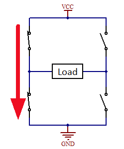
In practice the switches are usually implemented as some sort of transistors (bipolar, MOSFET or IGBT). The switches are closed diagonally (top left and lower right or top right and lower left) to connect the supply to the load in either direction. ChallengesThere are some challenges associated with H bridges. The two main ones are probably to avoid shoot-through and to drive the high side transistors. Shoot-through is the condition when either both of the left switches or both of the right switches are closed at the same time. This of course causes a short circuit which is a bad thing and can potentially destroy the switches or other components. Figure 2 illustrates the phenomenon. There are two plausible ways in which this can occur. One is that illegal control signals are applied, e.g. due to a software bug, and the other is that there is a short and unintentional overlap in the gate drive signals when switching from one polarity to the other.
Figure 2. The two left switches are accidentally on
at the same time causing a large short circuit current to flow.
The reason driving the high side transistors is a challenge is that they are referenced to a relatively high supply voltage instead of to ground while the control signals (typically coming from a micro controller or similar) are ground referenced. So some kind of level shifting circuitry is needed. Why build an H bridge?I had some odd 5-phase bipolar stepper motors (see separate article) lying around and just for fun I decided to design and build an H bridge that is suitable for driving these motors. A label on the motor says "Iw = 0.21 A, Rw = 32 ohms", so the H bridge needed to be able to support a drive voltage of 6.7 V. Factors that contributed to my decision to design and build an H bridge was that I had never done it before, I did not know beforehand exactly how to do it, the result would be at least a little interesting (a moving stepper motor) and it seemed like a reasonably small project that would be possible to complete with a limited amount of time and effort. Design choicesThe current of about 200 mA is not particularly high and it might be feasible to use bipolar transistors (BJTs) as switches. For higher currents, beefy power transistors with consequently lower current gain would have to be used and this would require a substantial base current, which can be a bit impractical to handle and cause a lot of loss and heat that needs to be dissipated. I decided to build the bridge with some margin on the current and voltage handling requirements and to use MOSFETs to avoid the problem of the power dissipation caused by the static base current of BJTs. NMOS transistors are about three times more efficient than PMOS transistors in terms of device size (cost) and gate capacitance for a given on-resistance, so for high-power designs it is advantageous to use NMOS transistors for both the upper and the lower switches. The problem with using NMOS transistors for the upper switches is however that they need a gate voltage that is higher than the bridge supply voltage. If PMOS transistors are used, gate voltages below the supply voltage are sufficient. For the convenience of avoiding an extra supply voltage and since the current is rather low and the cost of suitable PMOS transistors therefore not prohibitive, I decided to use PMOS transistors as the top switches and NMOS devices as the bottom ones. I wanted the design to be fail-safe in the sense that no combination or sequence of control signals could cause shoot-through so that bugs in the micro controller code would never be able to cause dangerous conditions. Two things are needed for this:
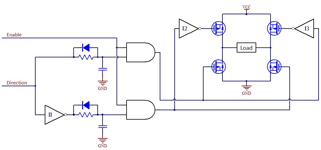
A conceptual solution that achieves the translation between the Enable/Direction control signals and the gate signals as well as introduces a delay when the transistors are about to turn on is shown in figure 3 below.
Figure 3. Conceptual diagram of how the gate drive
signals of the H bridge are generated. (Click on image to enlarge.)
The two AND gates allow the enable signal to disconnect the control signals from the gates of the MOSFETs. The diode/resistor combinations make the charging of the capacitors slower than the discharging so that it takes longer for the gate drive signals to reach the transistors when the transistors are about to turn on than when they are about to turn off. By letting the gate control signals from the AND gates control the transistors diagonally, a level change from one of the AND gates always either turns on or turns off both transistors that are controlled by the gate. This makes it possible to control the timing of the four transistors with just two delay circuits. The inverters I2 and I3 need to convert the logic levels from the AND gates to voltages suitable for driving the top transistors. Detailed designThere are many details to fill in to complete the design. Figure 4 below shows the full schematic that resulted from the design process. It can be useful to refer back to it when reading the sections below on how it came together.
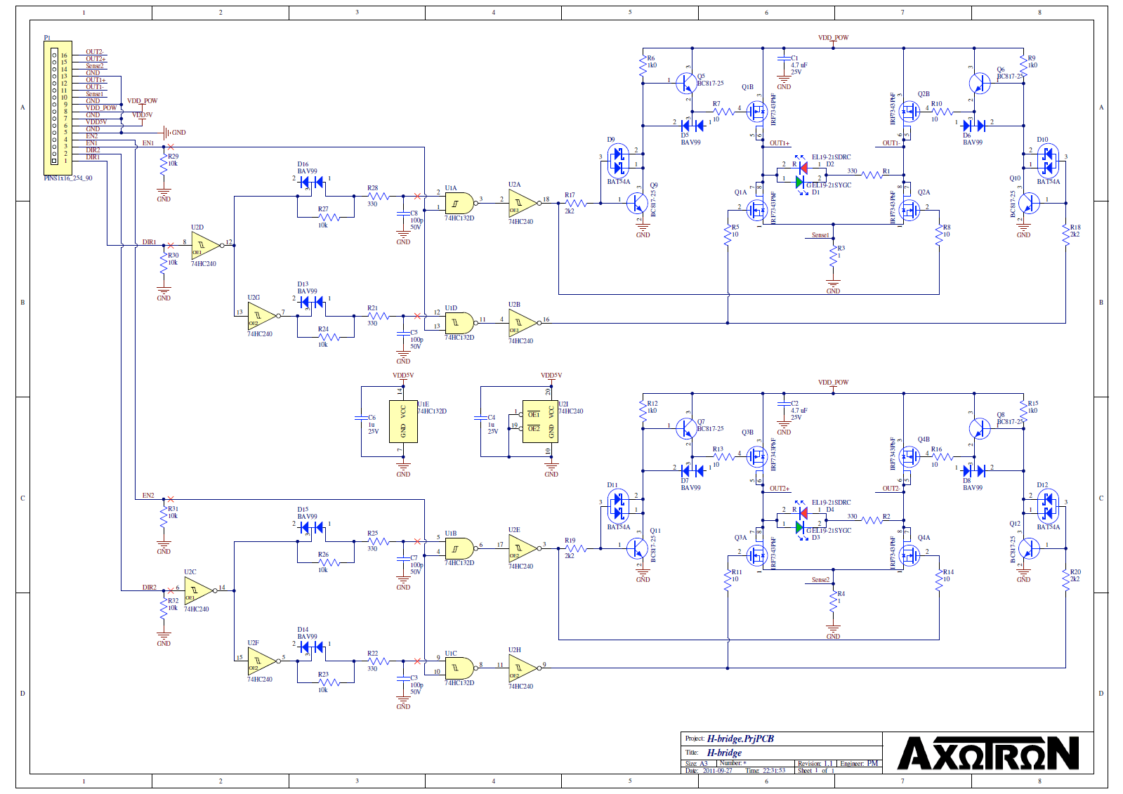
Figure 4. Schematic diagram of complete (dual) H
bridge. (Click on image to enlarge.)
Choice of logic gatesThe AND gates of figure 3 need to have Schmitt trigger inputs since they are driven by relatively slowly changing voltages. Unfortunately there are no AND Schmitt triggers available. Schmitt trigger NOR gates could be an alternative since both NOR and AND gates have a low output signal when they are disabled. Using NOR gates would make the enable signal active low, but that is no drawback. An advantage with using NOR gates is that the inverter I1 could be implemented by a NOR gate and then a single logic IC would suffice for the H bridge. As it turns out there are no NOR Schmitt triggers available either, so we are forced to use NAND Schmitt triggers (which do in fact exist). This means that we need to invert the outputs of the gates and while that could be done with the two other NAND gates in the same package we still need to implement the inverter I1 and preferably also have another buffer at the input of the Direction signal so that the external control signal does not have to drive the RC-link (we cannot be sure of the analog properties of the external Direction signal and we do not want the operation of the H bridge to be highly dependent upon the analog properties of a controlling signal. So we seem to need two logic ICs for the H bridge to give us the required two NAND gates and four inverters. There are however octal inverters available in the '240 series of logic circuits and together with a '32 quad NAND gate we have enough gates for two bridges. This is the reason I decided to build two bridges on the same board. Figure 5 below shows the resulting design.
Figure 5. Schematic diagram of the logic gates and
asymmetrical timing circuitry. (Click on image to enlarge.)
Several different logic families could have been used, but I wanted NAND gates that have CMOS input levels since that means that the Schmitt trigger inputs will switch at about half the supply voltage and I also want the inverters to have CMOS outputs to drive the gates of the NFETs up to about 5 V. So the NAND gates could be e.g. of the HC or AC families, whereas the inverters could be HC, HCT or AC etc. I decided to use HC for both. Using HCT for the inverter to also accommodate TTL levels on the Direction signal would not be a an advantage since the Enable signal does anyway have to have CMOS levels. Other input stage choicesI put pull-down resistors on the input signals to keep them at valid and safe (off) logic levels in case some input should at some time be left unconnected. CMOS inputs have very high impedance and can otherwise easily pick up noise that could cause a connected motor to go crazy. And it is generally good design practice to make modules robust anyway. I chose BAV99 for the diodes as this is an inexpensive diode I often use. In fact, BAV99 cnosists of two diodes in a SOT23 package so it may seem wasteful to buy two diodes and use only one of them. But instead of introducing another diode in the component library I decided to stick with an old and inexpensive one that I also happened to have in stock. To limit the current surge when the capacitors are to be charged, I put an extra 330 ohm resistor in series with the diode/resistor pair. The values of the other resistor and the capacitor were first approximately determined by hand calculation, then simulated using LTSpice and then fine tuned after the circuit had been built to make sure there is no shoot-through and a little margin. High side driverI found some inspiration in designing the H bridge in the following document from Texas Instruments:
None of the circuits in that document did however fit the bill perfectly for this project and I had to develop something else, partly based on ideas in the document. The driver circuit for the high side PMOS transistor needs to invert the signal and increase the swing to the supply voltage of the motor, which may be at least 7 V. It has to be able to charge and discharge the gate capacitance of the FET relatively quickly and pull it high with a low impedance when it is supposed to do so, so that the PFET stays off even though the parasitic gate-drain capacitance will act to pull it low when the lower NMOS transistor turns on and quickly pulls the drain voltage down.
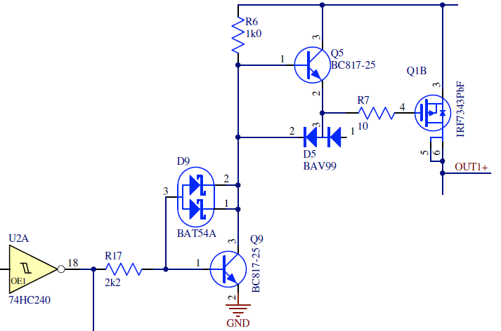
Figure 6. Schematic diagram of the high side driver.
(Click on image to enlarge.)
Figure 6 shows the finished driver circuit. The inversion and level shifting is handled by the NPN transistor Q9. This transistor would be very slow to turn off since it would be in saturation if it were not for the Schottky diode(s) from base to collector that prevents it from saturating. This is the same technique used internally in LSTTL logic to speed up the switching. I happened to have used the diode BAT54A before and decided to use it again. This is a dual diode and I put both diodes in parallel. Q5 is connected as an emitter follower and acts to provide the required low impedance to the supply rail when the PMOS transistor shall be off. Just relying on R6 to pull the gate high would have increased the time to pull the gate high (i.e. to turn off the transistor) substantially, but more importantly, the resistor would not have been able to keep the gate high when there is a quick drop (large negative dV/dt) at the drain of the PMOS transistor as a result of the lower NMOS turning on. The diode D5 provides a path for pulling the gate low when the PMOS is to turn on. A PNP emitter follower could have been used here to speed up the turn-on a bit, but we do intentionally slow down the turn-on anyway and the diode solution is fast enough. A small gate resistor R7 limits gate current surges and reduces the risk of ringing in the gate circuit. The rest of the circuitFigure 7 shows some other details of the bridge circuit.
Figure 7. Schematic of the low side driver and some
other details. (Click on image to enlarge.)
Driving the NMOS transistor is much simpler. A plain gate resistor (R8) is connected between the output of the inverter and the gate. I added a current sense resistor in the source leads of the NMOS transistors to be able to conveniently measure the current and verify that there is no shoot-through taking place. 1 ohm was selected as a compromise between getting a decent voltage to be measured by an oscilloscope and minimizing loss. At 0.2 A, we get 0.2 V drop and this is relatively insignificant compared to a supply voltage of 6 or 7 V. When the testing has been completed the 1-ohm resistor can be replaced by a 0-ohm resistor. For MOSFETs I selected IRF7343 which is an NMOS/PMOS combination in a single SO8 package. This selection was a compromise between price, availability and on-resistance. The maximum current the transistors support is much higher than what is required in this application, so if low cost were the main design goal; some other transistors would have been a better choice. Like most (all?) power MOSFETs, these transistors contain integral bulk diodes that are very useful in this application since they will take care of the current to discharge the motor winding when the bridge turns off. If bipolars had been used instead of MOSFETs, such diodes would have been necessary to add as discrete components to prevent damage to the transistors. I also added LEDs across the H bridge output. This gives a convenient visual indication of what the circuit is up to and can be very useful during development of any device making use of the bridge. For a finished product the LEDs might be better left out. I decided to put the dual H bridge circuit on a double sided PCB and pull out all the external signals to a one-row pin header, instead of designing a complete board with H bridge, micro controller, power supply etc. This minimized the effort required to finish the H bridge part of the project and it is always possible to integrate the H bridge together with more circuitry on a future board if that would become necessary. LayoutFigures 8 and 9 show the finished layout and figure 10 shows the assembly drawing. I like to work with surface mount components and all components except for the pin header are surface mount. The layout was done as a two layer board where most of the components are on the top layer and most of the bottom layer is a solid ground plane. Extensive gate and pin swapping was performed to simplify the layout and minimize the amount of tracks that would have to be placed on the bottom side and disrupt the ground plane. The pinout of the connector was also chosen to ease layout, but with signal and power integrity in mind.
Figure 8. The layout of the top and bottom layers.
(Click to enlarge.)
Figure 9. A 3D rendering of the H bridge PCBA.
(Click image to enlarge.)
Figure 10. The top assembly drawing.
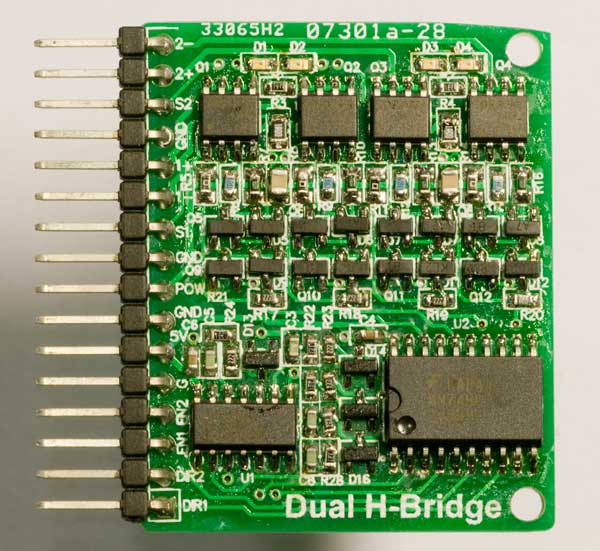
I think the layout turned out all right as it is compact and pretty much limited by the size of the connector and the area of the components. It is good for EMC (electromagnetic compatibility, i.e. the ability to not disturb and not be disturbed through electromagnetic fields) that the ground plane is kept quite solid. The components that were chosen are all relatively thin (U2 is thickest at about 2.7 mm maximum) so several boards can be stacked tightly together. The layout could however be made more compact if it were necessary. 0402 components could be chosen instead of 0603 and SC70/SOT323 packages might be available instead of the SOT23 packages that were used. U1 and U2 may also be available in smaller packages. I did however want to keep this design easy to assemble even without a microscope and that took priority over shrinking it further. PhotosThe PCB was manufactured (at ITead Studio) and I soldered the components to it manually. The result can be seen in figure 11 below.
Figure 11. A photo of the first H bridge that I
built.
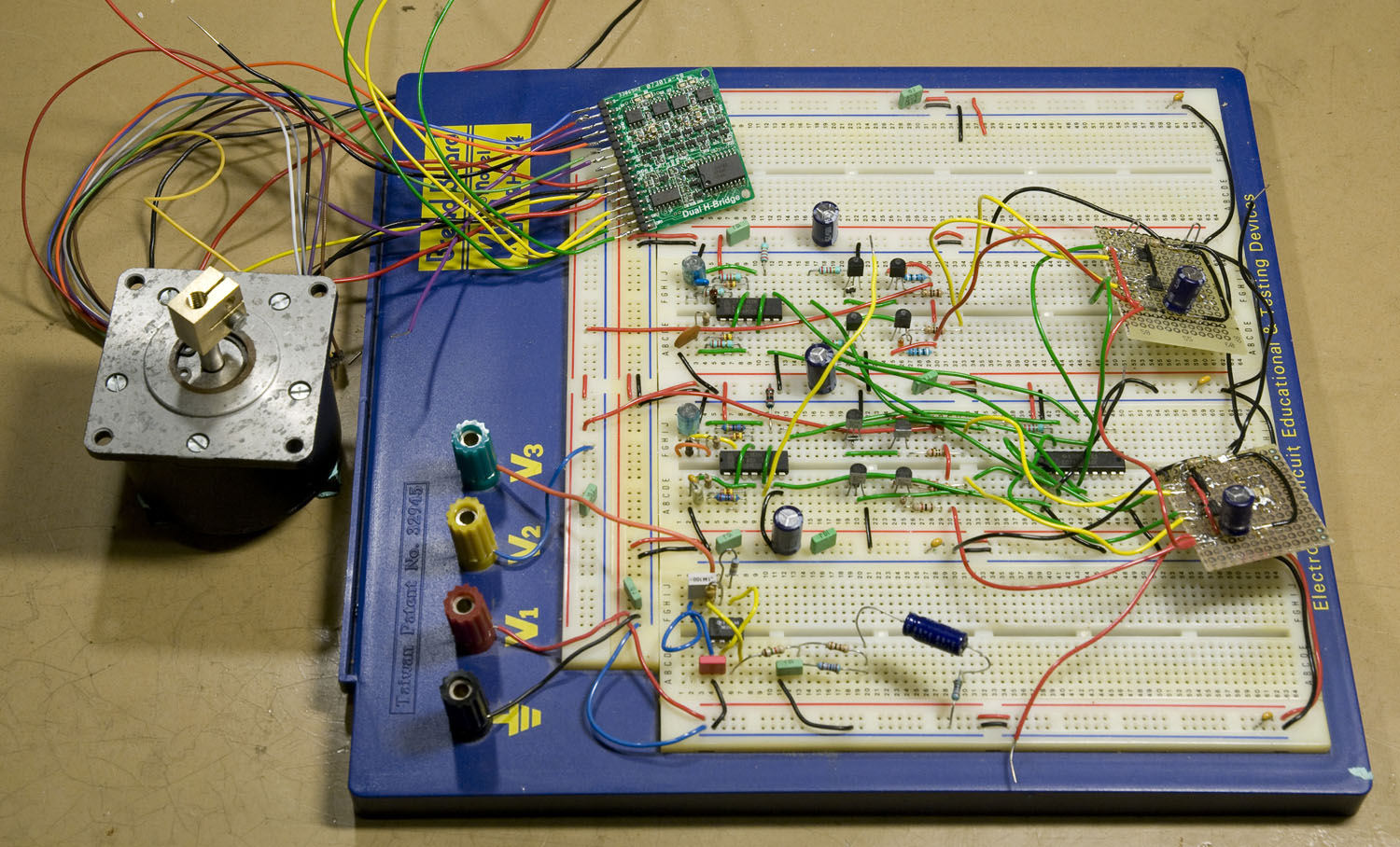
Unfortunately I had made a mistake in the design (the drive signals to the NMOS transistors were not cross connected as they should have been) and I needed to add four patch wires to the board to make it work (not shown in the photo). The schematic and layout files shown in the article do however have this mistake corrected. Before doing the layout of the H bridge and building it, I prototyped it all on a solderless breadboard (the surface mount MOSFETs I did however put on small PCB prototype boards since they do not lend themselves to direct connection to this kind of breadboard). The breadboard and the finished H bridge PCBA that replaced it is shown in figure 12 below.
Figure 12. Prototype board and finished dual H
bridge. (Click photo to enlarge.)
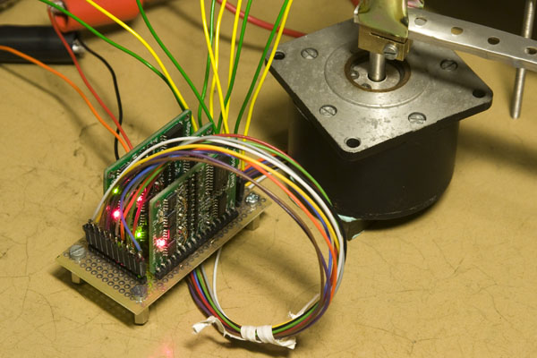
Figure 13 shows a photo of three dual H bridge boards driving one of the 5-phase bipolar stepper motors that I designed the bridge for.
Figure 13. H bridges driving a 5-phase bipolar
stepper motor.
A short movie clip showing three (of which two and a half are used) dual H bridges driving a 5-phase bipolar stepper motor is provided below.
Figure 14. Video showing H bridges driving a stepper
motor.
Oscilloscope plotsTo verify the operation of the H bridge (not the least to see that there is indeed no shoot-through), I looked at the gate voltages and the voltage drop over the current sense resistor using an oscilloscope. The resulting plots can be seen below. Unless something else is stated in the text the traces show the following signals:
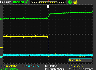
The blue and yellow curves both have their offsets set to one division above the bottom of the plots whereas the green trace has its zero level two divisions below the top. It can be helpful to refer to the schematic PDF to more easily follow the descriptions of the phenomena that are observed in the plots. NMOS turning on while PMOS is off
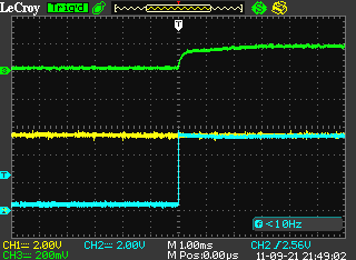
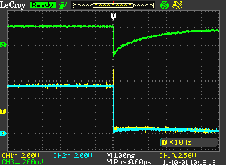
The NMOS transistor Q1A turns on while the PMOS Q1B
is off all the time, 250 ns/div and 1 ms/div.
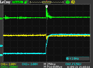
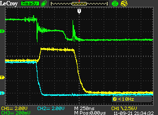
There is no sudden step in the current when the transistor turns on since the inductance of the motor winding prevents sudden changes in current. It takes ~400 µs for the current to rise to close to its final value. NMOS turning off while PMOS is off
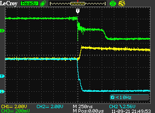
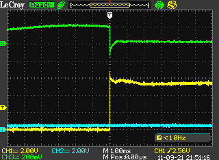
The NMOS transistor Q1A turns off while the PMOS Q1B
is off all the time, 250 ns/div and 1 ms/div.
Notice the ~400 µs long peak in the PMOS gate voltage after the NMOS turns off. What happens is that the NMOS stops conducting current, but the current in the large inductance of the motor continues to flow which very quickly raises the voltage at the drain of the PMOS until its body diode turns on. This sudden rise of the PMOS drain voltage couples into the gate of the PMOS through the gate-drain capacitance and raises the gate voltage. The emitter diode of Q5 is then back-biased and prevents the gate from being brought back to its original voltage. When the current in the winding has decayed to zero, the current also stops flowing in the body diode and the drain voltage suddenly goes down. This again couples to the gate which now returns to approximately its original voltage. Another phenomenon that can be observed is that the current through the sense resistor (green trace) first goes from 200 mA to 0 mA when the NMOS turns off and a little while later it goes to -200 mA and then decays slowly to 0. What happens here is that when the NMOS Q1A at the lower left turns off, the PMOS Q2B on the top right is still conducting since the PMOS drivers are slower than the NMOS drivers. As described above, the motor current starts flowing through the body diode of Q1B while it continues to flow through Q2B. During this period the current through the sense resistor is zero. 0.5 µs later the PMOS Q2B also turns off and the motor current needs to find another path. By sucking current from the drain node of the transistors to the right, the voltage at that node goes negative and current starts flowing through the body diode of Q2B until the current has decayed to zero, 400 µs later. PMOS turning on while NMOS is off
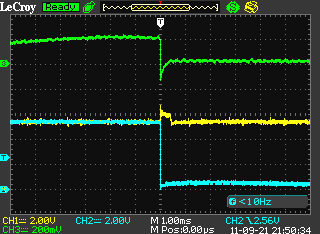
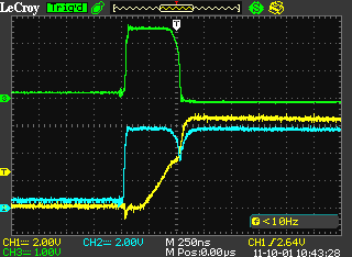
The PMOS transistor Q1B turns on while the NMOS Q1A is off
all the time, 250 ns/div and 1 ms/div
Notice the ~100 ns long plateau in the middle of the falling PMOS gate voltage. When the gate voltage of the PMOS falls, it quickly reaches the threshold voltage of the transistor and when that happens, the transistor starts conducting and quickly pulls the drain high. This rising drain voltage couples into the gate via the gate-drain capacitance and for a short while manages to counteract the current being pulled out of the gate capacitance via D5 and Q9. PMOS turning off while NMOS is off
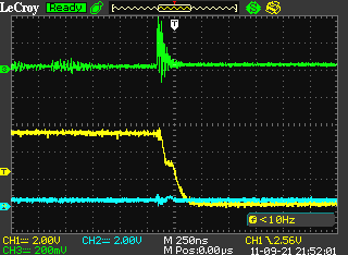
The PMOS transistor Q1B turns off while the NMOS Q1A is off
all the time, 250 ns/div and 1 ms/div
Here we see the same double-step behavior in the current through the sense resistor as we observed previously. The double step is again caused by the PMOS drivers being a little slower than the NMOS drivers. Here the NMOS transistor Q2A (whose gate voltage is not shown) turns off before the PMOS transistor turns off. That is the reason the current goes down to zero even before the PMOS gate voltage has changed at all. During this period when the sense voltage is zero, the current from the motor winding goes through the body diode of Q2B and the PMOS transistor Q1B which is still on. When the gate voltage of Q1B is high enough to reach the threshold voltage and it stops conducting, the current from the motor winding can no longer flow through the PMOS transistor Q1B and instead forces its drain voltage low until it starts pulling current through the body diode of Q1A. This is where the green trace (current) goes negative. The sudden step in drain voltage also couples through the parasitic gate-drain capacitance into the gate of the PMOS transistor Q1B and that is the reason for the plateau in the rising edge of the PMOS gate voltage trace. Polarity change, PMOS turning off, NMOS turning on
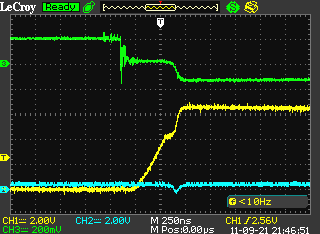
The PMOS transistor turns off and the NMOS turns on
(delayed by the asymmetrical delay circuit), 250 ns/div and 1 ms/div
The same thing happens here, namely that the NMOS transistor Q2A (whose gate voltage is not shown), turns off even before the gate voltage of PMOS Q1B starts changing and this is the reason the first thing that happens is that the current through the sense resistor initially goes to zero. The new thing here is that after the PMOS Q1B has turned off, NMOS Q1A turns on. The motor winding current then does not settle at zero once it has decayed, but instead builds up in the other direction than what it was first flowing in. It is a bit mysterious why it takes so much time (~5 ms) for the current to build up in this case whereas it took only a tenth of that time in the case above when the NMOS was turning on from a state where both transistors were off. The reason for the difference is probably that the motor was in different states when the two plots were taken. The position and movement of the rotor probably has an effect on the inductance and resistance of the windings (a device transforming electrical energy into mechanical energy must look at least somewhat resistive). Also, how the other windings are connected (or not) to the supply should matter. In the polarity reversal tests, the motor was driven in a way that all windings were powered at all times (except during the very brief period of polarity reversal), whereas in the on/off plots four of the windings were on and one was idle. This means that one winding was powered up and one was simultaneously powered down in those tests. Polarity change, NMOS turning off, PMOS turning on
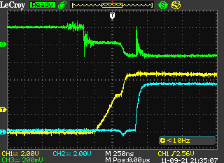
The NMOS transistor turns off and the PMOS turns on
(delayed by the asymmetrical delay circuit), 250 ns/div
Here we see a polarity reversal, but in the opposite direction. The phenomena that can be observed here have mostly been discussed above. One can note that since the PMOS driver is slower than the NMOS driver, there is a larger gap between the switching of the two transistors in this case. Shoot-through
By shorting D13, shoot-through can be observed when
the gate voltages of Q1A and Q1B are rising.
Avoiding shoot-through was one of the design goals and it can be seen from the plots above that no shoot-through occurs during switching. To illustrate what it would look like if there were shoot-through, I shorted D13 so that the asymmetrical timing circuits became symmetrical. The result can be seen in the plot above. Notice that I had to change the scale of the current sense waveform so that it is now 1 A/div. What happens when D13 is shorted is that the NMOS transistor Q1A (whose gate voltage is the blue curve) turns on before its companion PMOS Q1B (yellow) has turned off. This results in 2.5A of short circuit current during 0.5 µs. Files and referencesHere is a list of links to various design files. References
© Per Magnusson, Axotron |
![[PDF]](articles/H-Bridge/resources/pdf.png) The schematic as a PDF
The schematic as a PDF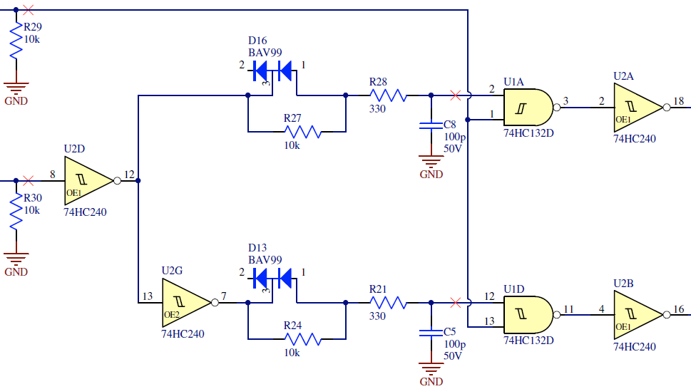


![[XLS]](articles/H-Bridge/resources/excel.png) Bill of materials
Bill of materials![[link]](articles/H-Bridge/resources/html.png) Wikipedia article on H bridges
Wikipedia article on H bridges| Updated: 2017-04-12, 21:33:55 |
|